| CPC H01L 25/0657 (2013.01) [G06F 3/0604 (2013.01); G06F 3/0655 (2013.01); G06F 3/0679 (2013.01); G06F 11/1068 (2013.01); G06F 12/0802 (2013.01); G06N 3/02 (2013.01); H01L 25/50 (2013.01); G06F 2212/60 (2013.01); G06F 2212/72 (2013.01); G11C 16/0483 (2013.01); H01L 2225/06513 (2013.01); H01L 2225/06541 (2013.01)] | 61 Claims |
|
1. An electronic device, comprising:
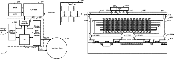
a memory circuit fabricated on a first semiconductor die, wherein the memory circuit comprises a quasi-volatile memory circuit that includes a plurality of modular memory units, each modular memory unit comprising (i) a three-dimensional array of storage transistors organized into a plurality of memory strings; and (ii) a group of conductors exposed to a surface of the first semiconductor die, the group of conductors being configured for communicating control, address and data signals associated the memory unit; and
a logic circuit fabricated on a second semiconductor die, wherein the logic circuit includes a plurality of conductors each exposed at a surface of the second semiconductor die, wherein the first and second semiconductor dies are wafer-bonded, such that the conductors exposed at the surface of the first semiconductor die are each electrically connected to a corresponding one of the conductors exposed to the surface of the second semiconductor die.
|