| CPC H01L 24/29 (2013.01) [B81C 1/00269 (2013.01); B81C 1/00293 (2013.01); H01L 23/10 (2013.01); H01L 23/49838 (2013.01); H01L 23/528 (2013.01); H01L 23/53228 (2013.01); H01L 23/53242 (2013.01); H01L 24/05 (2013.01); H01L 24/06 (2013.01); H01L 24/08 (2013.01); B81B 2207/012 (2013.01); B81C 2203/035 (2013.01); H01L 23/562 (2013.01); H01L 24/80 (2013.01); H01L 2224/05551 (2013.01); H01L 2224/05552 (2013.01); H01L 2224/05555 (2013.01); H01L 2224/05571 (2013.01); H01L 2224/05647 (2013.01); H01L 2224/05686 (2013.01); H01L 2224/06135 (2013.01); H01L 2224/06155 (2013.01); H01L 2224/06165 (2013.01); H01L 2224/06505 (2013.01); H01L 2224/08121 (2013.01); H01L 2224/08237 (2013.01); H01L 2224/29019 (2013.01); H01L 2224/8001 (2013.01); H01L 2224/80047 (2013.01); H01L 2224/80895 (2013.01); H01L 2224/80896 (2013.01); H01L 2224/80948 (2013.01); H05K 1/111 (2013.01)] | 23 Claims |
|
1. A bonded structure comprising:
a first semiconductor element including first conductive features and first non-conductive features;
a second semiconductor element including second conductive features and second non-conductive features, the second semiconductor element comprising an integrated device, the first semiconductor element directly bonded to the second semiconductor element such that the first conductive features are directly bonded to corresponding second conductive features without an intervening adhesive layer and the first non-conductive features are directly bonded to corresponding second non-conductive features without an intervening adhesive; and
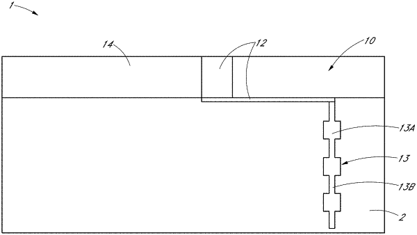
a crack stopper extending vertically through a portion of the second semiconductor element, the crack stopper including alternating wider and narrower segments.
|