| CPC H01L 24/05 (2013.01) [H01L 21/563 (2013.01); H01L 21/78 (2013.01); H01L 23/3142 (2013.01); H01L 24/03 (2013.01); H01L 24/16 (2013.01); H01L 24/32 (2013.01); H01L 24/73 (2013.01); H01L 24/81 (2013.01); H01L 24/83 (2013.01); H01L 24/92 (2013.01); H01L 24/96 (2013.01); H01L 25/105 (2013.01); H01L 21/568 (2013.01); H01L 21/76805 (2013.01); H01L 21/76816 (2013.01); H01L 21/76831 (2013.01); H01L 21/76832 (2013.01); H01L 23/485 (2013.01); H01L 24/11 (2013.01); H01L 24/13 (2013.01); H01L 2224/024 (2013.01); H01L 2224/0231 (2013.01); H01L 2224/02371 (2013.01); H01L 2224/03002 (2013.01); H01L 2224/0391 (2013.01); H01L 2224/0401 (2013.01); H01L 2224/05124 (2013.01); H01L 2224/05147 (2013.01); H01L 2224/1146 (2013.01); H01L 2224/11334 (2013.01); H01L 2224/11849 (2013.01); H01L 2224/13024 (2013.01); H01L 2224/16145 (2013.01); H01L 2224/32145 (2013.01); H01L 2224/73204 (2013.01); H01L 2224/831 (2013.01); H01L 2224/92125 (2013.01); H01L 2225/1023 (2013.01); H01L 2225/1058 (2013.01); H01L 2924/3512 (2013.01)] | 19 Claims |
|
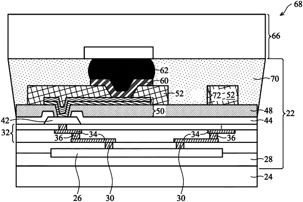
1. A method comprising:
forming a first redistribution line and a second redistribution line, both extending into a first dielectric layer;
forming a second dielectric layer covering the first redistribution line and the second redistribution line;
patterning the second dielectric layer to form a first dielectric island and a second dielectric island, wherein the first dielectric island covers the first redistribution line, and the second dielectric island covers the second redistribution line, wherein after the second dielectric layer is patterned, a remaining portion of the second dielectric layer forms a dielectric strip joining both of the first dielectric island and the second dielectric island, and wherein a combined part of the second dielectric layer comprising the first dielectric island, the second dielectric island, and the dielectric strip is physically separated from other parts of the second dielectric layer; and
forming a first Under-Bump Metallurgy (UBM) and a second UBM extending into the first dielectric island and the second dielectric island, respectively.
|