| CPC H01L 23/66 (2013.01) [H03F 1/086 (2013.01); H03F 3/195 (2013.01); H01L 2223/6616 (2013.01); H01L 2223/6655 (2013.01); H03F 2200/451 (2013.01)] | 21 Claims |
|
1. A transistor amplifier, comprising:
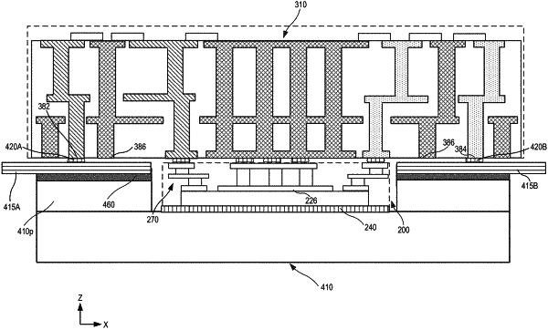
a group III-nitride based amplifier die comprising a gate terminal, a drain terminal, and a source terminal on a first surface of the amplifier die; and
an interconnect structure electrically bonded to the gate terminal, drain terminal and source terminal of the amplifier die on the first surface of the amplifier die and electrically bonded to an input path and output path of the transistor amplifier by respective conductive bonding elements that are external to the amplifier die,
wherein the interconnect structure comprises a circuitry module including gate, drain, and source connection pads having respective surfaces that are exposed at a first side of the circuitry module facing the first surface of the amplifier die, and the respective surfaces of the gate, drain, and source connection pads are electrically bonded to the gate, drain, and source terminals, respectively, by the respective conductive bonding elements.
|