| CPC H01L 23/535 (2013.01) [H01L 23/53276 (2013.01)] | 20 Claims |
|
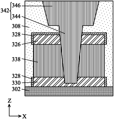
1. An interconnection structure, comprising:
a first conductive feature comprising a two-dimensional material layer, a first conductive layer disposed on the two-dimensional material layer, and a second conductive layer, wherein the two-dimensional material layer is disposed on the second conductive layer;
a second conductive feature disposed over the first conductive feature and through the first conductive layer, the two-dimensional material layer, and in the second conductive layer; and
a dielectric material disposed adjacent the first and second conductive features.
|