| CPC H01L 23/528 (2013.01) [H01L 23/5226 (2013.01); H01L 29/0649 (2013.01)] | 16 Claims |
|
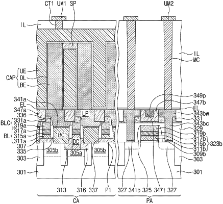
1. A semiconductor device, comprising:
a semiconductor substrate including a first region and a second region;
a first interlayer insulating layer covering the second region;
a capping layer disposed on the first interlayer insulating layer, wherein an upper surface of the capping layer includes a first trench;
conductive patterns spaced apart on the capping layer, wherein side surfaces of the conductive patterns are aligned with inner side surfaces of the first trench; and
a peripheral separation pattern disposed in the first trench to cover the side surfaces of the conductive patterns,
wherein the peripheral separation pattern has a first thickness on the side surfaces of the conductive patterns and a second thickness greater than or equal to the first thickness on a lower surface of the first trench.
|