| CPC H01L 23/528 (2013.01) [H01L 21/02568 (2013.01); H01L 21/47635 (2013.01); H01L 21/76802 (2013.01); H01L 23/5226 (2013.01); H01L 23/535 (2013.01); H01L 27/124 (2013.01); H01L 27/1222 (2013.01); H01L 27/1259 (2013.01); H01L 29/24 (2013.01); H01L 29/41733 (2013.01); H01L 29/42392 (2013.01); H01L 29/66969 (2013.01); H01L 29/78642 (2013.01); G05B 2219/1163 (2013.01)] | 13 Claims |
|
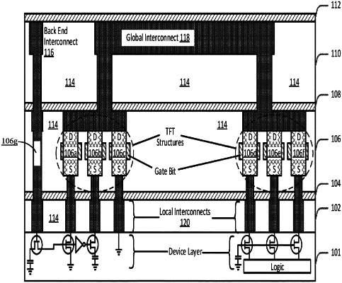
1. An integrated circuit structure, comprising:
a plurality of first interconnect features;
a plurality of second interconnect features;
a third interconnect feature;
a first plurality of selectable vias, each of the first plurality of selectable vias comprising a corresponding first thin film transistor (TFT) structure, the first TFT structure including a first gate electrode, a first source contact, and a first drain contact, wherein one of the first source contact or the first drain contact is connected to a corresponding one of the plurality of first interconnect features, and the other one of the first source contact or the first drain contact is connected to the third interconnect feature, and the first gate electrode is configured to receive a first select signal that causes the corresponding one of the plurality of first interconnect features to be electrically connected to the third interconnect feature; and
a second plurality of selectable vias, each of the second plurality of selectable vias comprising a second thin film transistor (TFT) structure, the second TFT structure including a second gate electrode, a second source contact, and a second drain contact, wherein one of the second source contact or the second drain contact is connected to a corresponding one of the plurality of second interconnect features, and the other one of the second source contact or the second drain contact is connected to the third interconnect feature, and the second gate electrode is configured to receive a second select signal that causes the corresponding one of the plurality of second interconnect features to be electrically connected to the third interconnect feature, wherein the third interconnect feature vertically overlaps and extends between the other one of the second source contact or the second drain contact of each of the second TFT structures and the other one of the first source contact or the first drain contact of each of the first TFT structures, and wherein the third interconnect feature electrically couples the other one of the second source contact or the second drain contact of each of the second TFT structures and the other one of the first source contact or the first drain contact of each of the first TFT structures.
|