| CPC H01L 23/5227 (2013.01) [H01F 27/2823 (2013.01); H01F 27/32 (2013.01); H01L 23/5329 (2013.01); H01L 23/53223 (2013.01); H01L 23/53238 (2013.01); H01L 28/10 (2013.01)] | 16 Claims |
|
1. An integrated circuit (IC) device, comprising:
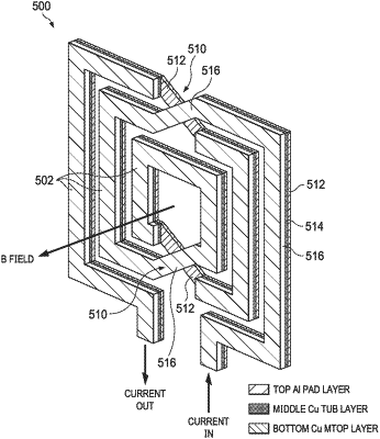
an IC structure including an integrated inductor;
wherein the integrated inductor comprises an elongated inductor wire defined by a metal layer stack including an upper metal layer, a middle metal layer, and a lower metal layer; and
wherein a lateral width of the middle metal layer of the inductor wire is greater than 1 μm; and
wherein the middle metal layer of the inductor wire is formed in a common layer with at least one metal via distinct from the integrated inductor.
|