| CPC H01L 23/5223 (2013.01) [H01L 28/90 (2013.01)] | 17 Claims |
|
1. A structure comprising:
a bottom electrode located on a surface of an interconnect level, the bottom electrode having a base portion and a via portion that extends upward from a surface of the base portion;
a capacitor high-k dielectric material layer located on the base portion of the bottom electrode;
a high-k dielectric material spacer located along an entirety of a sidewall of the via portion of the bottom electrode, wherein the high-k dielectric material spacer and the capacitor high-k dielectric material layer are composed of a compositionally same high-k dielectric material, and wherein the high-k dielectric material spacer has a topmost surface that is coplanar with a topmost surface of the via portion of the bottom electrode and is entirely spaced apart from the capacitor high-k dielectric material layer;
a top electrode located on the capacitor high-k dielectric material layer;
a first contact structure contacting the via portion of the bottom electrode; and
a second contact structure contacting the top electrode.
|
|
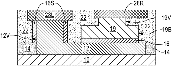
10. A structure comprising:
a bottom electrode located on a surface of an interconnect level, the bottom electrode having a base portion and a via portion that extends upward from a surface of the base portion;
a capacitor high-k dielectric material layer located on the base portion of the bottom electrode;
a high-k dielectric material spacer located along an entirety of a sidewall of the via portion of the bottom electrode, wherein the high-k dielectric material spacer and the capacitor high-k dielectric material layer are composed of a compositionally same high-k dielectric material, and wherein the high-k dielectric material spacer has a topmost surface that is coplanar with a topmost surface of the via portion of the bottom electrode and is entirely spaced apart from the capacitor high-k dielectric material layer;
a top electrode located on the capacitor high-k dielectric material layer, the top electrode having a base portion and a via portion that extends upward from a surface of the base portion;
a first contact structure contacting the via portion of the bottom electrode; and
a second contact structure contacting the via portion of the top electrode.
|
|
14. A structure comprising:
a bottom electrode located on a surface of an interconnect level;
a capacitor high-k dielectric material layer located on the bottom electrode;
a top electrode located on the capacitor high-k dielectric material layer, the top electrode having a base portion and a via portion that extends upward from a surface of the base portion;
a first contact structure directly contacting the bottom electrode; and
a second contact structure contacting the via portion of the top electrode, wherein the capacitor high-k dielectric material layer is located entirely above a topmost surface of the bottom electrode and is laterally spaced apart from the first contact structure.
|