| CPC H01L 23/49827 (2013.01) [H01L 23/13 (2013.01); H01L 23/367 (2013.01); H01L 23/49838 (2013.01); H01L 24/32 (2013.01); H01L 24/73 (2013.01); H01L 25/165 (2013.01); H01L 25/167 (2013.01); H01S 5/0234 (2021.01); H01S 5/02253 (2021.01); H01S 5/02469 (2013.01); H05K 1/112 (2013.01); H05K 1/181 (2013.01); H01L 2224/32227 (2013.01); H01L 2224/73265 (2013.01)] | 20 Claims |

|
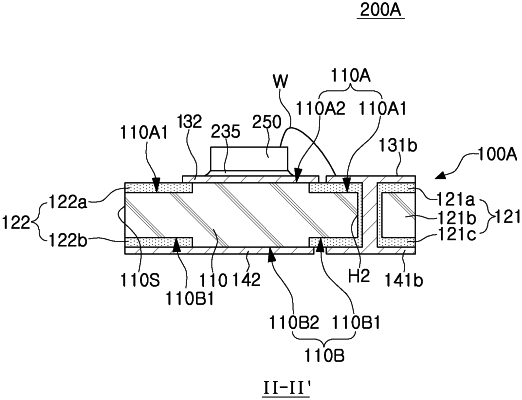
1. A wiring board comprising:
a metal plate having first and second surfaces opposite to each other, and having at least one through-hole penetrating through the first and second surfaces;
at least one conductive via respectively disposed in the at least one through-hole and spaced apart from the metal plate;
an insulating structure comprising at least one through-insulating portion disposed between the at least one through-hole and the conductive via, and a first insulating layer and a second insulating layer extending from the at least one through-insulating portion and disposed in a first region of the first surface of the metal plate, on the first surface and the second surface, respectively, wherein the first insulating layer comprises an upper surface substantially coplanar with a surface of a second region of the first surface where the insulating structure is not formed;
at least one first upper pad disposed on the first insulating layer and electrically connected to the conductive via;
at least one first lower pad disposed on the second insulating layer and electrically connected to the conductive via;
a second upper pad disposed on the first surface of the metal plate; and
a second lower pad disposed on the second surface of the metal plate and electrically connected to the second upper pad through the metal plate.
|