| CPC H01L 23/49811 (2013.01) [H01L 21/02274 (2013.01); H01L 21/486 (2013.01); H01L 23/53219 (2013.01); H01L 23/53233 (2013.01); H01L 23/53295 (2013.01)] | 20 Claims |
|
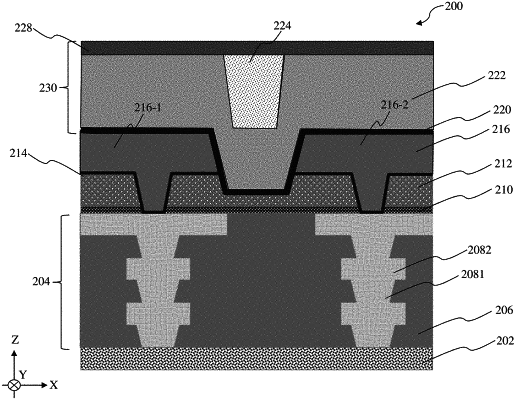
1. A semiconductor device, comprising:
a redistribution layer comprising:
a passivation layer, and
a first conductive feature and a second conductive feature disposed in the passivation layer;
a first contact feature disposed over and electrically coupled to the first conductive feature;
a second contact feature disposed over and electrically coupled to the second conductive feature; and
a passivation feature extending from between the first conductive feature and the second conductive feature to between the first contact feature and the second contact feature, the passivation feature comprising:
a dielectric feature including a planar top surface extending from a first end of the passivation feature adjacent the first contact feature to a second end of the passivation feature adjacent the second contact feature, and
a dielectric layer disposed on the planar top surface of the dielectric feature,
wherein a composition of the dielectric feature is different from a composition of the dielectric layer,
wherein the passivation feature partially extends into the passivation layer.
|