| CPC H01L 23/49548 (2013.01) [H01L 21/4825 (2013.01); H01L 21/4842 (2013.01); H01L 21/561 (2013.01); H01L 21/78 (2013.01); H01L 23/3121 (2013.01); H01L 23/49582 (2013.01); H01L 24/48 (2013.01); H01L 24/97 (2013.01); H01L 24/16 (2013.01); H01L 2224/16245 (2013.01); H01L 2224/48091 (2013.01); H01L 2224/48106 (2013.01); H01L 2224/48247 (2013.01)] | 13 Claims |
|
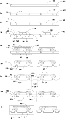
1. A semiconductor chip package device, comprising:
a lead frame, chips, an encapsulating layer, and an electroplating layer, wherein:
the lead frame includes a first surface, a second surface, first grooves extending from the first surface to the second surface, second grooves extending from the second surface towards the first surface and having a recessed surface between, and in parallel with, the first and second surfaces, and third grooves extending from the second surface towards the first surface, wherein the first grooves are connected to the second grooves and the third grooves are disposed at edges of the lead frame;
the chips are electrically connected to the lead frame;
the encapsulating layer is formed by using an encapsulating material to encapsulate at least a portion of the first surface of the lead frame and the chips, wherein the first grooves are filled with the encapsulating material, the encapsulating material in each of the first grooves passes through the lead frame and protrudes into a corresponding second groove, with the protruded encapsulating material protruding under the recessed surface of the second groove by a distance; and
the electroplating layer is disposed on the second surface of the lead frame, and extends into the third grooves or into the third grooves and the second grooves.
|