US 11,670,570 B2
Electronic device and method of manufacturing an electronic device
Yusuf Cinar, Yongin-si (KR); Jaehong Park, Suwon-si (KR); Seongyun Baek, Suwon-si (KR); and Hanhong Lee, Suwon-si (KR)
Assigned to SAMSUNG ELECTRONICS CO., LTD., Gyeonggi-Do (KR)
Filed by Samsung Electronics Co., Ltd., Suwon-si (KR)
Filed on May 8, 2020, as Appl. No. 16/870,068.
Claims priority of application No. 10-2019-0059920 (KR), filed on May 22, 2019; and application No. 10-2019-0084219 (KR), filed on Jul. 12, 2019.
Prior Publication US 2020/0373221 A1, Nov. 26, 2020
Int. Cl. H01L 23/427 (2006.01); H01L 23/00 (2006.01); H01L 25/065 (2023.01); H01L 21/52 (2006.01); H01L 21/48 (2006.01)
CPC H01L 23/427 (2013.01) [H01L 21/4871 (2013.01); H01L 21/52 (2013.01); H01L 24/32 (2013.01); H01L 24/83 (2013.01); H01L 25/0655 (2013.01); H01L 2224/32245 (2013.01); H01L 2924/1443 (2013.01)] 20 Claims
OG exemplary drawing
 
1. An electronic device comprising:
a substrate;
at least one electronic element on the substrate;
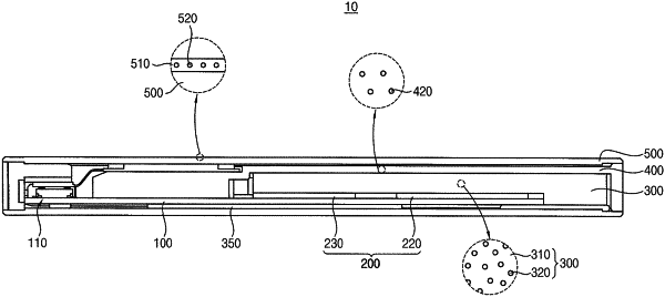
a heat dissipating pad on the substrate in thermal contact with the at least one electronic element, and including an encapsulated phase change material therein; and
a bracket covering the substrate, the at least one electronic element and the heat dissipating pad, the bracket directly contacting the substrate and the heat dissipating pad.