| CPC H01L 23/42 (2013.01) [H01L 23/3737 (2013.01); H01L 24/17 (2013.01); H01L 2924/15311 (2013.01)] | 22 Claims |
|
1. An integrated circuit (IC) package, comprising:
a package substrate;
a die; and
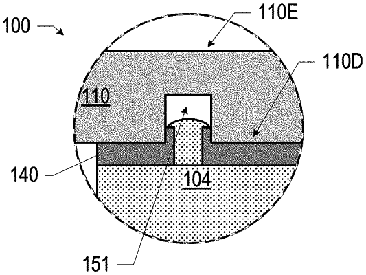
a lid including a bottom surface and a top surface, wherein the die is between the package substrate and the lid, the bottom surface of the lid is between the die and the top surface of the lid, and the bottom surface of the lid includes a channel that at least partially overlaps the die, wherein the lid further includes a first material, an adhesion material on at least a portion of a bottom surface of the first material, and a second material at a bottom of the channel, wherein the channel is in the bottom surface of the first material, wherein the second material has a different material composition than the first material, and wherein the second material separates the bottom of the channel and the adhesion material.
|