| CPC H01L 23/3675 (2013.01) [H01L 24/32 (2013.01); H01L 25/0655 (2013.01); H01L 23/367 (2013.01); H01L 25/50 (2013.01); H01L 2224/32237 (2013.01); H01L 2924/3511 (2013.01)] | 20 Claims |
|
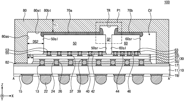
1. A semiconductor package, comprising:
a first substrate;
a first chip structure and a second chip structure spaced apart from each other on the first substrate, a gap region being defined between the first and second chip structures; and
a heat dissipation member covering the first chip structure, the second chip structure, and the first substrate, the heat dissipation member including a first trench in an inner top surface of the heat dissipation member,
wherein the first trench vertically overlaps with the gap region, a width between directly facing inner sidewalls of the first trench being greater than a width of the gap region, and
wherein the first trench vertically overlaps with at least a portion of a top surface of the first chip structure or a portion of a top surface of the second chip structure.
|