| CPC H01L 23/367 (2013.01) [H01L 21/4853 (2013.01); H01L 21/4857 (2013.01); H01L 21/4871 (2013.01); H01L 21/565 (2013.01); H01L 23/3185 (2013.01); H01L 23/49816 (2013.01); H01L 23/49822 (2013.01); H01L 24/16 (2013.01); H01L 2224/16227 (2013.01); H01L 2924/15311 (2013.01); H01L 2924/18161 (2013.01)] | 17 Claims |
|
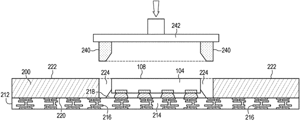
1. A method of making a semiconductor device, comprising:
providing a substrate;
providing a heat spreader including an opening formed through the heat spreader;
disposing a semiconductor die over the substrate;
disposing the heat spreader over the substrate with the semiconductor die in the opening; and
disposing a thermally conductive material in the opening between the heat spreader and semiconductor die, wherein the thermally conductive material is a preformed elastomer plug.
|