| CPC H01L 23/3171 (2013.01) [H01L 23/3192 (2013.01); H01L 23/528 (2013.01); H01L 21/78 (2013.01); H01L 23/291 (2013.01); H01L 23/296 (2013.01); H01L 23/585 (2013.01); H01L 24/05 (2013.01); H01L 2224/0219 (2013.01); H01L 2224/0221 (2013.01); H01L 2224/02181 (2013.01); H01L 2224/05541 (2013.01); H01L 2224/05553 (2013.01)] | 20 Claims |
|
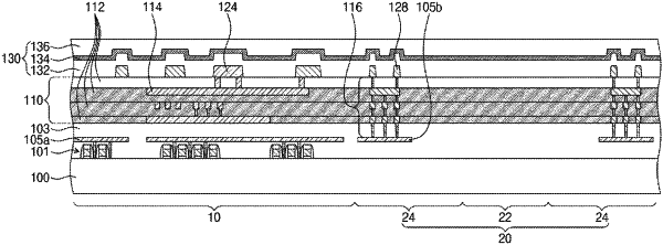
1. A semiconductor device, comprising:
a substrate including a chip region and an edge region around the chip region;
integrated circuit elements on the chip region;
an interlayer insulating layer covering the integrated circuit elements;
an interconnection structure having internal interconnection lines on the interlayer insulating layer, the interconnection structure having a side surface on the edge region;
a first conductive pattern and a second conductive pattern on the interconnection structure, wherein the first conductive pattern and the second conductive pattern are each electrically connected to the internal interconnection lines, wherein the first conductive pattern and the second conductive pattern are laterally spaced apart from each other in a direction parallel to a top surface of the substrate, and wherein the first conductive pattern has a bottom surface that is on a same vertical level as a bottom surface of the second conductive pattern;
a first passivation layer covering the first conductive pattern and the second conductive pattern and the side surface of the interconnection structure; and
a second passivation layer on the first passivation layer,
wherein:
the second passivation layer includes a second insulating material, the first passivation layer includes a first insulating material, and the second insulating material of the second passivation layer is different from the first insulating material of the first passivation layer, and
in a region between the first conductive pattern and the second conductive pattern, the second passivation layer has a bottom surface that is located at a vertical level lower than a top surface of the first conductive pattern.
|