| CPC H01L 22/32 (2013.01) [H01L 21/4853 (2013.01); H01L 21/4857 (2013.01); H01L 21/565 (2013.01); H01L 22/12 (2013.01); H01L 23/3128 (2013.01); H01L 23/5383 (2013.01); H01L 23/5386 (2013.01); H01L 23/5389 (2013.01); H01L 24/19 (2013.01); H01L 24/20 (2013.01); H01L 24/48 (2013.01); H01L 2224/214 (2013.01); H01L 2224/48227 (2013.01)] | 20 Claims |
|
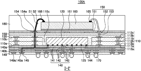
1. A semiconductor package, comprising:
a first connection structure having a first surface and a second surface opposing the first surface, the first connection structure comprising a first redistribution structure including a first redistribution layer and a first redistribution via;
a first semiconductor chip on the first surface of the first connection structure and comprising a first connection pad electrically connected to the first redistribution structure;
a second connection structure on the first semiconductor chip and comprising a second redistribution structure including a second redistribution layer and a second redistribution via;
a vertical connection structure on at least one side of the first semiconductor chip and electrically connecting the first redistribution structure and the second redistribution structure;
a first pad and a second pad on the second surface of the first connection structure and electrically connected to the second redistribution structure;
a first passivation layer on the second surface of the first connection structure and having a plurality of openings, the first and second pads being accessible via the plurality of openings;
a second semiconductor chip on the second connection structure and comprising a second connection pad electrically connected to the second redistribution structure through a bonding wire; and
an electrical connection metal only on the first pad,
wherein the first and second redistribution structures and the vertical connection structure provide a control signal path electrically connecting the first connection pad of the first semiconductor chip and the second connection pad of the second semiconductor chip and a test signal path electrically connecting the second connection pad of the second semiconductor chip and the second pad.
|