| CPC H01L 22/32 (2013.01) [G01R 31/2884 (2013.01); H01L 23/562 (2013.01); H01L 23/564 (2013.01); H01L 23/585 (2013.01)] | 24 Claims |
|
1. A wafer comprising a plurality of dies including a first die and a second die adjacent to or in proximity of the first die, wherein:
the first die comprises a device under test configured to receive radio frequency (RF) test signals through a wafer probe for wafer testing, the wafer probe including traces to conduct the RF test signals; and
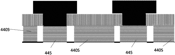
the second die comprises test pads, circuits and a patterned metal layer patterned to electrically shield the traces conducting the RF test signals applied to the first die from the circuits in the second die, the test pads being electrically isolated from the patterned metal layer.
|