US 11,670,553 B2
Gate stack treatment
Chandrashekhar Prakash Savant, Hsinchu (TW); Chia-Ming Tsai, Hsinchu (TW); Ming-Te Chen, Hsinchu (TW); Shih-Chi Lin, Hsinchu (TW); Zack Chong, Hsinchu (TW); and Tien-Wei Yu, Hsinchu (TW)
Assigned to Taiwan Semiconductor Manufacturing Co., Ltd., Hsinchu (TW)
Filed by Taiwan Semiconductor Manufacturing Co., Ltd., Hsinchu (TW)
Filed on Aug. 9, 2021, as Appl. No. 17/397,529.
Application 17/397,529 is a division of application No. 16/376,432, filed on Apr. 5, 2019, granted, now 11,088,029.
Claims priority of provisional application 62/736,766, filed on Sep. 26, 2018.
Prior Publication US 2021/0366778 A1, Nov. 25, 2021
Int. Cl. H01L 21/8234 (2006.01); H01L 21/28 (2006.01); H01L 29/66 (2006.01); H01L 21/768 (2006.01); H01L 27/088 (2006.01); H01L 29/78 (2006.01); H01L 29/49 (2006.01); H01L 21/324 (2006.01)
CPC H01L 21/823437 (2013.01) [H01L 21/28088 (2013.01); H01L 21/28158 (2013.01); H01L 21/324 (2013.01); H01L 21/76832 (2013.01); H01L 21/823431 (2013.01); H01L 21/823462 (2013.01); H01L 27/0886 (2013.01); H01L 29/4966 (2013.01); H01L 29/66795 (2013.01); H01L 29/785 (2013.01)] 20 Claims
OG exemplary drawing
 
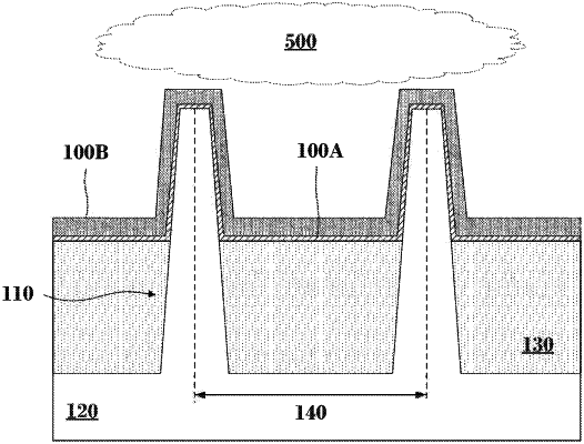
1. A method, comprising:
forming a fin on a substrate;
forming a gate dielectric stack on the fin, wherein the gate dielectric stack comprises a high-k dielectric layer disposed on an interfacial dielectric layer;
exposing a surface of the high-k dielectric layer to a fluorine-based gas.