| CPC H01L 21/78 (2013.01) [H01L 21/76838 (2013.01); H01L 23/544 (2013.01)] | 20 Claims |
|
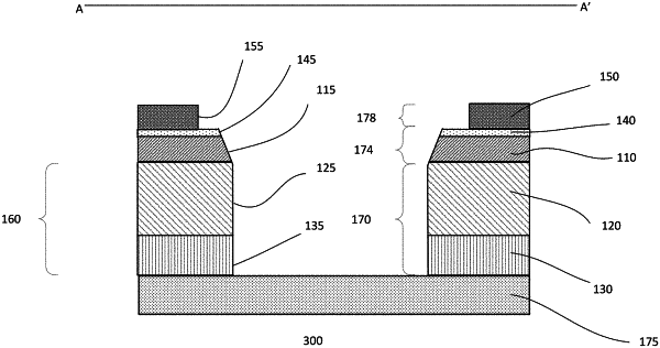
1. A method for forming a device comprising:
providing a wafer with a front surface and a back surface, the front surface includes a plurality of dies, wherein the wafer includes defined saw streets in first and second orthogonal directions between rows and columns of dies;
forming backside metallization (BSM) over the back surface of the wafer, wherein forming the BSM comprises selectively forming the BSM layer on the back surface of the wafer, wherein the selectively formed BSM layer is formed on the back surface of the wafer except in the saw streets, exposing the saw streets; and
etching the wafer from the back surface of the wafer using the selectively formed BSM layer as an etch mask to singulate the wafer into individual dies, wherein etching the wafer from the back surface forms wafer sidewalls with slanted wafer sidewall surfaces.
|