| CPC H01L 21/76832 (2013.01) [H01L 21/31116 (2013.01); H01L 21/31144 (2013.01); H01L 21/76802 (2013.01); H01L 21/76826 (2013.01); H01L 21/76828 (2013.01); H01L 21/76843 (2013.01); H01L 21/76877 (2013.01); H01L 23/5226 (2013.01); H01L 23/53238 (2013.01)] | 20 Claims |
|
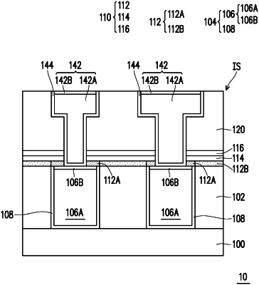
8. A semiconductor structure, comprising:
a substrate; and
an interconnect structure disposed over the substrate, the interconnect structure comprising interlayer dielectric layers, an etch stop layer between two of the interlayer dielectric layers and conductive features embedded in the interlayer dielectric layers, wherein the etch stop layer comprises an insulating layer and a silicon-containing insulating layer over the insulating layer, the insulating layer comprises a metal oxide region covering at least one of the interlayer dielectric layers and at least one metal nitride region covering the conductive features.
|