| CPC H01L 21/76802 (2013.01) [H01L 21/4853 (2013.01); H01L 21/76841 (2013.01)] | 20 Claims |
|
1. A method of manufacturing a semiconductor device, the method comprising:
forming a first photoresist material over a seed layer;
exposing the first photoresist material through a phase shift mask;
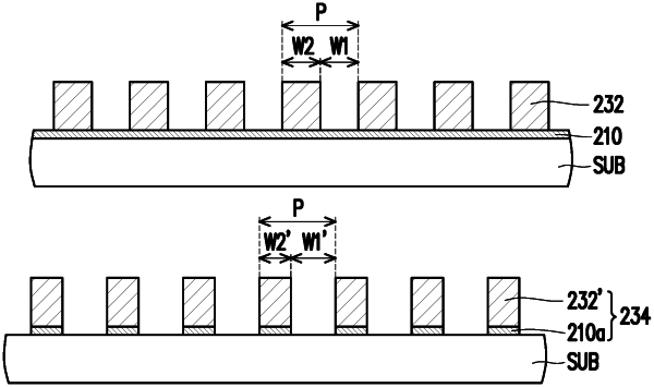
developing the first photoresist material to form a first photoresist layer, wherein the first photoresist layer comprises a plurality of first photoresist patterns and a plurality of first openings between the plurality of first photoresist patterns;
forming a first conductive material in the plurality of first openings;
forming a second photoresist layer over the first conductive material, wherein the second photoresist layer comprises at least one second opening;
forming a second conductive material in the at least one second opening;
removing the first photoresist layer and the second photoresist layer, to form a plurality of first conductive patterns and at least one second conductive pattern; and
using the plurality of first conductive patterns as a mask, partially removing the seed layer, to form a plurality of seed layer patterns under the plurality of first conductive patterns.
|