| CPC H01L 21/76202 (2013.01) [H01L 21/76224 (2013.01); H01L 21/76243 (2013.01); H01L 27/10861 (2013.01); H01L 27/10876 (2013.01)] | 21 Claims |
|
1. A semiconductor device comprising:
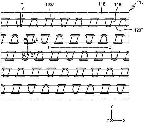
a substrate including an active region defined by a device isolation film;
a gate trench disposed in the substrate and crossing the active region and the device isolation film in a first direction that is parallel to a top surface of the substrate;
a gate insulating layer disposed in the gate trench; and
a gate electrode disposed on the gate insulating layer and fully buried in the gate trench,
wherein the gate electrode includes a first portion and a plurality of second portions disposed at a plurality of portions of a side of the first portion,
wherein the first portion of the gate electrode crosses the active region and the device isolation film in the first direction,
wherein the plurality of second portions of the gate electrode are disposed on the device isolation film and extend from the plurality of portions of the side of the first portion of the gate electrode in a second direction that is perpendicular to the first direction, and
wherein a bottom surface of the gate insulating layer is rounded, when viewed in a cross-section in the second direction.
|