| CPC H01L 21/02032 (2013.01) [B32B 43/006 (2013.01); H01L 21/02079 (2013.01); H01L 21/67092 (2013.01); H01L 22/12 (2013.01); H01L 24/799 (2013.01); H01L 24/98 (2013.01); B32B 2457/14 (2013.01)] | 20 Claims |
|
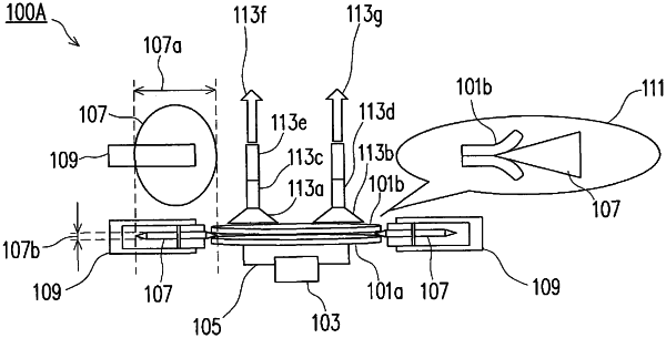
1. A debonding system for debonding a pair of bonded wafers, comprising:
a wafer chuck having a preset maximum lateral dimension and configured to rotate the pair of bonded wafers attached to a top surface of the wafer chuck;
a pair of circular plate separating blades including a first separating blade and a second separating blade arranged diametrically opposite to each other at edges of the pair of bonded wafers,
wherein the first and the second separating blades are inserted between a first and a second wafers of the pair of bonded wafers; and
at least two pulling heads configured to pull the second wafer upwardly so as to debond the second wafer from the first wafer.
|