| CPC H01L 21/4853 (2013.01) [H01L 21/486 (2013.01); H01L 21/4857 (2013.01); H01L 21/568 (2013.01); H01L 21/6835 (2013.01); H01L 23/3185 (2013.01); H01L 23/49816 (2013.01); H01L 23/49894 (2013.01); H01L 23/5383 (2013.01); H01L 23/5386 (2013.01); H01L 24/05 (2013.01); H01L 24/16 (2013.01); H01L 24/32 (2013.01); H01L 24/73 (2013.01); H01L 25/0655 (2013.01); H01L 25/18 (2013.01); H01L 24/81 (2013.01); H01L 24/83 (2013.01); H01L 24/92 (2013.01); H01L 2221/68345 (2013.01); H01L 2221/68359 (2013.01); H01L 2221/68372 (2013.01); H01L 2224/0401 (2013.01); H01L 2224/05571 (2013.01); H01L 2224/16227 (2013.01); H01L 2224/16238 (2013.01); H01L 2224/32225 (2013.01); H01L 2224/73204 (2013.01); H01L 2224/81005 (2013.01); H01L 2224/83005 (2013.01); H01L 2924/1432 (2013.01); H01L 2924/1434 (2013.01)] | 20 Claims |
|
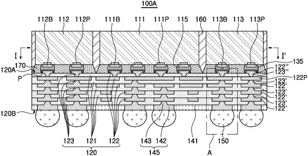
1. A method of manufacturing a semiconductor package, the method comprising:
forming a base insulating layer on a first carrier substrate;
forming a planar conductive pattern on the base insulating layer;
forming a redistribution structure on the base insulating layer, wherein the redistribution structure includes a plurality of insulating layers, and a plurality of redistribution layers between the plurality of insulating layers, respectively, each of the plurality of redistribution layers having a conductive via connected to an adjacent one of planar conductive pattern and the plurality of redistribution layers;
forming an underbump metallurgy (UBM) pad on an upper surface of the redistribution structure, the UBM pad having a UBM via connected to an uppermost redistribution layer among the plurality of redistribution layers;
attaching a second carrier substrate to the upper surface of the redistribution structure, on which the UBM pad is formed, so that the redistribution structure is provided between the first carrier substrate and the second carrier substrate;
removing the first carrier substrate from the base insulating layer; and
forming a connection pad on the base insulating layer, the connection pad having a connection via penetrating through the base insulating layer and connected to the planar conductive pattern.
|