| CPC H01L 21/31116 (2013.01) [H01L 21/02063 (2013.01); H01L 21/31144 (2013.01)] | 20 Claims |
|
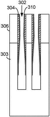
1. A method of forming an etched feature in a dielectric-containing stack on a substrate, the method comprising:
(a) partially etching the feature in the dielectric-containing stack by exposing the substrate to a first plasma comprising an etching reactant;
(b) after (a), depositing a protective film on sidewalls of the feature, the protective film comprising at least one of a tungsten carbonitride, a tungsten sulfide, tin, a tin-containing compound, molybdenum, a molybdenum-containing compound, a ruthenium sulfide, an aluminum sulfide, zirconium, and a zirconium-containing compound, wherein the protective film is not deposited on bottoms of the etch features; and
(c) repeating (a)-(b) until the feature is etched to a final depth, wherein the protective film deposited in (b) substantially prevents lateral etch of the feature during (a), and wherein the feature has an aspect ratio of about 5 or greater at its final depth.
|