| CPC H01L 21/28176 (2013.01) [H01L 21/28035 (2013.01); H01L 21/823857 (2013.01); H01L 29/401 (2013.01); H01L 29/4236 (2013.01); H01L 29/42368 (2013.01); H01L 29/4983 (2013.01); H01L 29/66568 (2013.01); H01L 29/7856 (2013.01)] | 10 Claims |
|
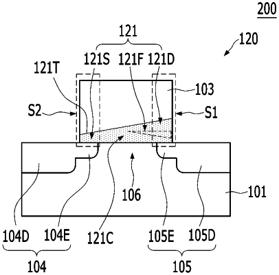
1. A semiconductor device, comprising:
a gate structure including a dielectric material over a substrate and a columnar crystal grain material over the dielectric material, the gate structure including a source side and a drain side;
an oxidation promotion species doped on the drain side of the gate structure to increase a thickness of the dielectric material on the drain side of the gate structure; and
a source region and a drain region formed in the substrate,
wherein the source region and the drain region are formed to laterally extend to overlap with the source side and the drain side of the gate structure, respectively,
wherein the dielectric material of the gate structure has a thickness that gradually and continuously increases from the source side of the gate structure toward the drain side of the gate structure.
|