| CPC H01L 21/0337 (2013.01) [H01L 21/31144 (2013.01); H01L 21/32139 (2013.01); H01L 21/76816 (2013.01); H01L 23/528 (2013.01); H01L 21/0274 (2013.01); H01L 21/28123 (2013.01); H01L 21/31 (2013.01); H01L 21/76897 (2013.01); H01L 45/1675 (2013.01); H01L 51/0018 (2013.01); H01L 2224/0362 (2013.01); H01L 2224/11622 (2013.01)] | 18 Claims |
|
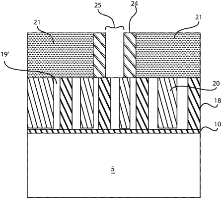
1. A method of forming a semiconductor integrated circuit, the method comprising:
providing a substantially planar structure comprising a plurality of first spacers comprising a spacer material, wherein alternating first and second regions between the first spacers are respectively filled with a first material and a second material, and wherein the first spacers extend laterally in a first direction parallel to a substrate;
patterning a masking layer on the substantially planar structure to define an opening, wherein the opening has a first width in a second direction such that a first portion of a central first spacer and a second portion of an adjacent first spacer are both exposed, and wherein (i) the second direction is perpendicular to the first direction and (ii) the second direction is parallel to the substrate;
forming second spacers on opposing sidewalls of the opening, such that a width of the opening is reduced in the first and second directions such that the only exposed spacer material in the opening comprises a third portion of the central first spacer; and
removing the spacer material of the third portion of the central first spacer.
|