| CPC H01L 21/02631 (2013.01) [H01L 21/0262 (2013.01); H01L 21/02263 (2013.01); H01L 21/02554 (2013.01); H01L 22/12 (2013.01)] | 18 Claims |
|
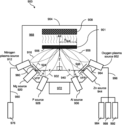
1. A material deposition system comprising:
a rotation mechanism that rotates a substrate deposition plane of a substrate around a center axis of the substrate deposition plane;
a heater configured to heat the substrate;
a material source that supplies a material to the substrate, wherein the material source has i) an exit aperture with an exit aperture plane and ii) a predetermined material ejection spatial distribution from the exit aperture plane, the predetermined material ejection spatial distribution having a symmetry axis which intersects the substrate at a point offset from the center axis, wherein the exit aperture is positioned at an orthogonal distance, a lateral distance, and a tilt angle relative to the center axis of the substrate; and
a positioning mechanism that allows dynamic adjusting of the orthogonal distance, the lateral distance, or the tilt angle;
wherein the dynamic adjusting is based on a desired layer uniformity for a desired layer growth rate.
|