| CPC H01L 21/02529 (2013.01) [C01B 32/956 (2017.08); C23C 16/325 (2013.01); C30B 25/20 (2013.01); C30B 29/36 (2013.01); H01L 21/02378 (2013.01); H01L 21/02428 (2013.01); H01L 21/02634 (2013.01); H01L 29/04 (2013.01); H01L 29/1608 (2013.01); H01L 29/34 (2013.01); C01B 32/90 (2017.08)] | 9 Claims |
|
1. A SiC epitaxial wafer comprising:
a 4H-SiC single crystal substrate which has
a surface with an off angle with respect to a c-plane as a main surface and
a bevel part on a peripheral part; and
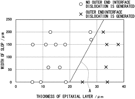
a SiC epitaxial film having a film thickness of 20 μm or more, which is formed on the 4H-SiC single crystal substrate,
wherein a density of an interface dislocation extending from an outer peripheral edge of the SiC epitaxial layer is 10 lines/cm or less.
|