| CPC H01G 4/1227 (2013.01) [H01G 4/012 (2013.01); H01G 4/248 (2013.01); H01G 4/30 (2013.01)] | 20 Claims |
|
1. A multilayer ceramic capacitor, comprising:
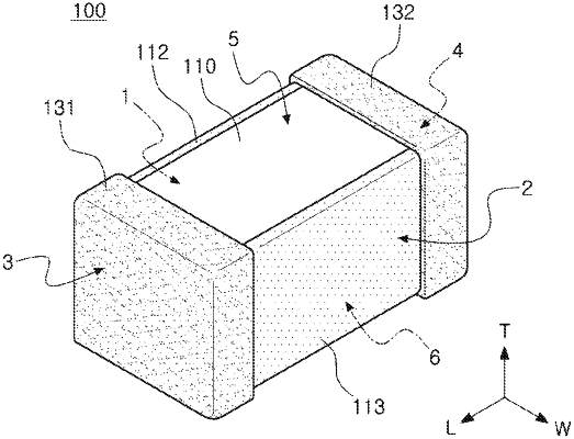
a ceramic body comprising a dielectric layer, and a first surface and a second surface opposing each other, a third surface and a fourth surface connecting the first and second surfaces, and a fifth surface and a sixth surface connected to the first to fourth surfaces and opposing each other;
a plurality of internal electrodes disposed in the ceramic body, exposed on the first and second surfaces, and each having one end exposed through one of the third surface or the fourth surface; and
a first side margin portion and a second side margin portion arranged on end portions of the internal electrodes exposed through the first and second surfaces, respectively,
wherein the ceramic body comprises an active portion comprising the plurality of internal electrodes arranged to overlap each other with the dielectric layer interposed therebetween to form capacitance, and cover portions disposed above an uppermost internal electrode and below a lowermost internal electrode of the active portion,
the first and second side margin portions comprise tin (Sn), and a content of the tin (Sn) included in the first and second side margin portions is greater than a content of tin (Sn) included in the dielectric layer of the active portion, and
an average size of dielectric grains included in the first and second margin portions is smaller than an average size of dielectric grains included in the dielectric layer of the active portion.
|