| CPC H01B 7/0045 (2013.01) [B29C 64/10 (2017.08); B29C 64/106 (2017.08); B33Y 10/00 (2014.12); B33Y 30/00 (2014.12); B33Y 80/00 (2014.12); B60R 16/0207 (2013.01); H01B 7/009 (2013.01); H01B 7/0275 (2013.01); H01B 7/363 (2013.01); H01B 7/40 (2013.01); H01B 13/0013 (2013.01); H01B 13/01209 (2013.01); H01B 13/01236 (2013.01); H01B 13/01263 (2013.01); H01B 13/24 (2013.01); H01R 12/592 (2013.01); H01R 12/675 (2013.01); H01R 13/502 (2013.01); H01R 27/02 (2013.01); H05K 3/00 (2013.01); H01B 13/01254 (2013.01); H01R 13/5202 (2013.01); H01R 13/5205 (2013.01); H01R 2201/26 (2013.01)] | 19 Claims |
|
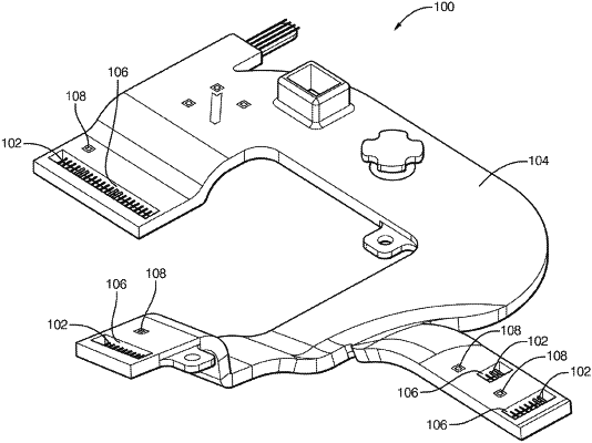
1. A method of manufacturing a wiring harness assembly, comprising:
forming a plurality of electrically conductive wires encased within a substrate formed of a dielectric material;
forming an opening in the substrate located and sized such that a section of the plurality of electrically conductive wires is exposed within the opening;
disposing a support segment within the opening;
securing a connector segment including a plurality of terminals to the support segment; and
placing the plurality of terminals in mechanical and electrical contact with the plurality of electrically conductive wires, wherein the method employs an apparatus to perform the steps of forming the plurality of electrically conductive wires encased within the substrate formed of the dielectric material and forming the opening in the substrate such that the section of the plurality of electrically conductive wires is exposed within the opening, the apparatus comprising:
an extruding device configured to selectively dispense a dielectric material though an orifice;
a wire feed device configured to selectively feed a conductive wire through the orifice:
a cutting device configured to selectively sever the conductive wire after it is fed through the orifice; and
an electronic controller configured to control the extruding device, the wire feed device, and the cutting device.
|