| CPC G11C 17/165 (2013.01) [G11C 17/18 (2013.01)] | 22 Claims |
|
1. A re-programmable integrated circuit, comprising:
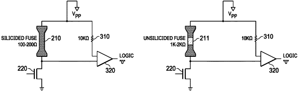
a plurality of non-volatile memory elements, each memory element including an electrically conductive fuse portion in an initial state, the initial state being either a first initial state having a first resistance value or a second initial state having a second resistance value;
re-programming circuitry for altering the state of each of said non-volatile memory elements, said re-programming circuitry including a controllable element coupled to the fuse portion of each memory element, each said controllable element selectively operable to cause an electrical current to flow through said fuse portion sufficient to cause that fuse portion to transition to an altered state having a third resistance value greater than said first and second resistance values;
reference resistance circuitry comprising a reference selection switch configurable between an initial programmed state and a re-programmed state, said reference selection switch configured in said initial programmed state prior to altering the programmed state of each of said non-volatile memory elements and in said re-programmed state after altering the initial programmed state of any of said non-volatile memory elements, wherein a reference resistance of said reference resistance circuitry is a first reference value when said reference selection switch is in said initial programmed state and a second reference value when said reference selection switch is in said re-programmed state; and,
read circuitry for determining the logic state of each of said non-volatile memory elements, said read circuitry comprising a comparator circuit operable to sense the resistance value of the electrically conductive fuse portion of a memory element and said reference resistance, wherein the logic state of a memory element is a function of whether the resistance value of the memory element is greater than or less than said reference resistance.
|