| CPC G11C 16/32 (2013.01) [G11C 16/10 (2013.01)] | 20 Claims |
|
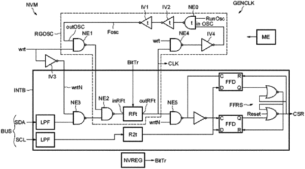
1. A method for writing to an electrically erasable and programmable non-volatile memory, the method comprising:
operatively connecting a filter circuit belonging to a communication interface to an oscillator circuit, wherein the communication interface is physically connected to a bus, and wherein operatively connecting the filter circuit comprises transitioning the filter circuit from a disabled state to an enabled state, the enabled state comprising enabling access to functions of the filter circuit, the disabled state comprising a bypass mode corresponding to the filter circuit being non-operational and the oscillator circuit receiving a valid signal;
generating, by the oscillator circuit, an oscillation signal by accumulating elementary delays; and
regulating the oscillation signal by the filter circuit to generate a clock signal for timing a write cycle, the regulating comprising inserting an additional delay equal to a time constant of the filter circuit into the accumulation of elementary delays, the accumulation of elementary delays being negligible in duration with respect to the additional delay.
|