| CPC G11C 16/26 (2013.01) [G11C 11/5642 (2013.01); G11C 11/5671 (2013.01); G11C 16/0483 (2013.01); G11C 16/08 (2013.01); G11C 16/24 (2013.01); G11C 16/30 (2013.01)] | 12 Claims |
|
1. A semiconductor memory comprising:
a plurality of memory cell transistors, a threshold voltage of each of the memory cell transistors being changeable to store multi-bit data;
a word line which is electrically connected to gates of the memory cell transistors;
a plurality of bit lines which are electrically connected to one ends of the memory cell transistors, respectively;
a source line which is electrically connected to the other ends of the memory cell transistors;
a plurality of sense amplifier units which are electrically connected to the bit lines, respectively, each of the sense amplifier units including a sense amplifier, a first latch, and a second latch; and
a controller,
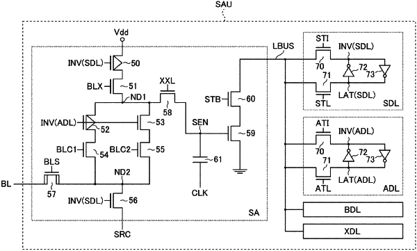
wherein each of the sense amplifiers includes
a first transistor having a gate to which a first control signal is supplied, and one end electrically connected to a corresponding one of the bit lines,
a second transistor having a gate to which a second control signal is supplied, one end electrically connected to the other end of the first transistor, and the other end electrically connected to a first node,
a third transistor having a gate to which a third control signal is supplied, and one end electrically connected to the first node,
a fourth transistor having a gate to which a signal based on data stored in a corresponding one of the first latches is supplied, one end electrically connected to the other end of the third transistor, and the other end electrically connected to a first power supply node,
a fifth transistor having a gate to which a fourth control signal is supplied and one end electrically connected to the first node, and
a sixth transistor having a gate to which a signal based on data stored in a corresponding one of the second latches is supplied, one end electrically connected to the other end of the fifth transistor, and the other end electrically connected to a second power supply node.
|