| CPC G11C 16/26 (2013.01) [G11C 16/0483 (2013.01); G11C 16/08 (2013.01); G11C 16/24 (2013.01); H01L 27/1157 (2013.01); H01L 27/11519 (2013.01); H01L 27/11524 (2013.01); H01L 27/11529 (2013.01); H01L 27/11556 (2013.01); H01L 27/11565 (2013.01); H01L 27/11573 (2013.01); H01L 27/11582 (2013.01)] | 21 Claims |

|
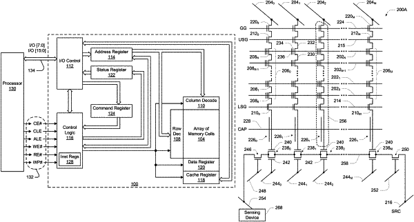
1. An array of memory cells, comprising:
a data line;
a source;
a plurality of pass gates connected in series between the data line and the source, wherein each pass gate of the plurality of pass gates comprises a first channel, a second channel, a first control gate capacitively coupled to its first channel, a second control gate capacitively coupled to its second channel, a first source/drain region connected to its first channel and to its second channel, and a second source/drain region connected to its first channel and to its second channel;
a plurality of unit column structures, wherein each unit column structure of the plurality of unit column structures comprises a respective plurality of series-connected non-volatile memory cells connected in series with a respective plurality of series-connected field-effect transistors, wherein a channel of each non-volatile memory cell of the plurality of series-connected non-volatile memory cells and a channel of each field-effect transistor of the plurality of series-connected field-effect transistors are selectively connected to one another; and
a plurality of backside gate lines, wherein each backside gate line is connected to the second control gate of a respective pass gate of the plurality of pass gates;
wherein, for each unit column structure of the plurality of unit column structures, the channel of a particular field-effect transistor of its respective plurality of field-effect transistors is capacitively coupled to the first channel of a respective pass gate of the plurality of pass gates.
|