| CPC G11C 16/24 (2013.01) [G11C 16/0483 (2013.01); G11C 16/10 (2013.01); H01L 27/11556 (2013.01); H01L 27/11582 (2013.01); H01L 27/11519 (2013.01); H01L 27/11565 (2013.01)] | 19 Claims |
|
1. A memory device comprising:
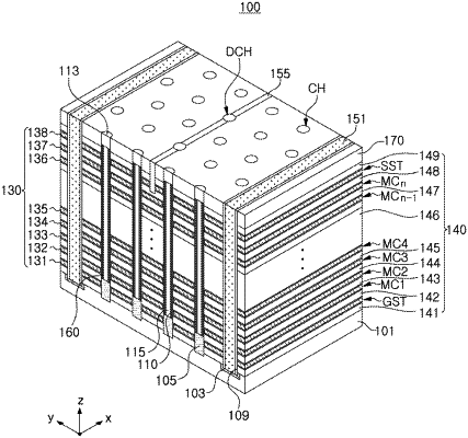
a stacked structure disposed on a substrate, wherein the stacked structure comprises a plurality of gate electrode layers alternating with a plurality of insulating layers;
one or more channel structures penetrating through the stacked structure, wherein the channel structures are disposed on an epitaxial layer connected to the substrate; and
a wordline cut region dividing the stacked structure into a plurality of regions,
wherein the gate electrode layers comprise a ground select line, a string select line, and a plurality of wordlines disposed between the ground select line and the string select line,
the wordlines and the channel structures adjacent to the wordlines provide memory cells, and
a thickness of each of the wordlines decreases and a bitline voltage input to a bitline connected to the memory cells decreases as a distance from the wordline cut region increases.
|