| CPC G11C 16/08 (2013.01) [G11C 5/06 (2013.01); G11C 16/102 (2013.01); G11C 16/26 (2013.01); G11C 16/30 (2013.01)] | 13 Claims |
|
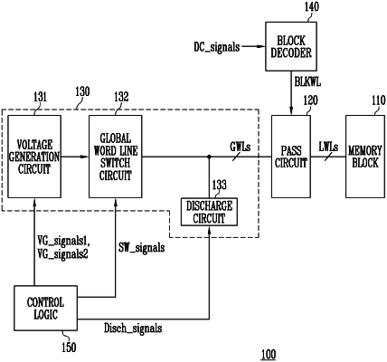
1. A semiconductor memory device comprising:
a memory block including a plurality of memory cells connected to local word lines;
a pass circuit including transistors configured to, in response to a block selection signal, connect or disconnect between the local word lines and global word lines; and
a voltage providing circuit configured to apply an operation voltage of a program operation or a read operation to the global word lines while the transistors connect between the local word lines and the global word lines,
wherein the transistors are configured to disconnect between the local word lines and the global word lines after the program operation or the read operation is completed, and
wherein the voltage providing circuit is configured to discharge the global word lines while the transistors disconnect between the local word lines and the global word lines.
|