| CPC G11C 11/4085 (2013.01) [G11C 11/4076 (2013.01); G11C 11/4091 (2013.01); G11C 11/4094 (2013.01); G11C 11/4096 (2013.01); G11C 16/3404 (2013.01); H03K 19/01742 (2013.01)] | 20 Claims |

|
1. An integrated circuit, comprising:
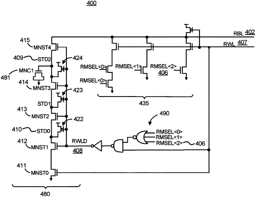
a memory cell array coupled to a bitline and a first wordline; and
an NMOS pull-down structure coupled to the bitline and a plurality of PMOS transistors,
wherein:
the plurality of PMOS transistors is coupled to a second wordline, a logic value carried on the second wordline based on a logic value carried on the first wordline, and structured to pre-charge a plurality of drains of the NMOS pull-down structure to a high logic value based on a low logic value carried on the second wordline, and
the NMOS pull-down structure discharges the bitline based on a high logic value carried on the second wordline.
|