US 11,670,359 B2
Semiconductor memory device capable of operating at high speed, low power environment by optimizing latency of read command and write command depending on various operation modes
Woongrae Kim, Gyeonggi-do (KR)
Assigned to SK hynix Inc., Gyeonggi-do (KR)
Filed by SK hynix Inc., Gyeonggi-do (KR)
Filed on May 25, 2022, as Appl. No. 17/824,470.
Application 17/824,470 is a division of application No. 17/097,151, filed on Nov. 13, 2020, granted, now 11,404,104.
Claims priority of application No. 10-2020-0077046 (KR), filed on Jun. 24, 2020.
Prior Publication US 2022/0284943 A1, Sep. 8, 2022
This patent is subject to a terminal disclaimer.
Int. Cl. G11C 7/22 (2006.01); G11C 11/4076 (2006.01); G11C 11/4096 (2006.01); G11C 11/408 (2006.01)
CPC G11C 11/4076 (2013.01) [G11C 11/4082 (2013.01); G11C 11/4087 (2013.01); G11C 11/4096 (2013.01)] 16 Claims
OG exemplary drawing
 
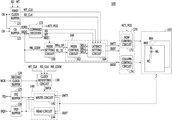
1. A latency setting circuit, comprising:
a clock driving circuit configured to delay a first operating clock by a latency corresponding to an activated one of a plurality of mode selection signals for setting different latencies to generate a first trigger signal, during a first operation; and
a first latency circuit configured to delay a first operating command and latch the first operating command according to the first trigger signal provided from the clock driving circuit to output a first internal command.