US 11,670,358 B2
Memory with adjustable TSV delay
John H. Gentry, Boise, ID (US); Michael J. Scott, Boise, ID (US); Greg S. Gatlin, Mountain Home, ID (US); Lael H. Matthews, Meridian, ID (US); Anthony M. Geidl, Boise, ID (US); Michael Roth, Boise, ID (US); Markus H. Geiger, Boise, ID (US); Dale H. Hiscock, Boise, ID (US); and Evan C. Pearson, Boise, ID (US)
Assigned to Micron Technology, Inc., Boise, ID (US)
Filed by Micron Technology, Inc., Boise, ID (US)
Filed on Oct. 7, 2021, as Appl. No. 17/496,728.
Application 17/496,728 is a continuation of application No. 16/706,548, filed on Dec. 6, 2019, granted, now 11,145,352.
Prior Publication US 2022/0028443 A1, Jan. 27, 2022
This patent is subject to a terminal disclaimer.
Int. Cl. G11C 7/00 (2006.01); G11C 11/4076 (2006.01); H01L 25/065 (2023.01)
CPC G11C 11/4076 (2013.01) [H01L 25/0657 (2013.01); H01L 2225/06541 (2013.01)] 20 Claims
OG exemplary drawing
 
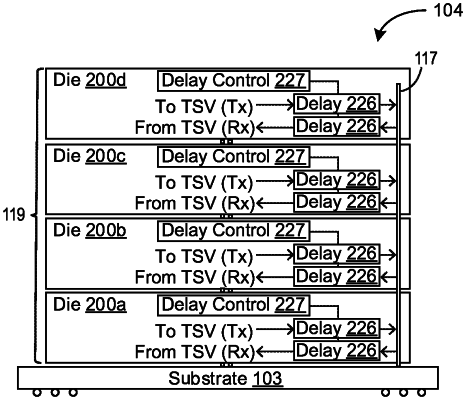
1. A memory die, comprising:
first circuitry coupled to a through-silicon via (TSV) that is configured to transmit signals to or receive signals from the memory die, the first circuitry configured to introduce propagation delay onto first signals transmitted to or received from the TSV at only the memory die; and
second circuitry configured, based at least in part on internal timings of second signals transmitted to or received from the TSV at another memory die, to adjust the propagation delay by activating the first circuitry, deactivating the first circuitry, or adjusting the first circuitry.