| CPC G11C 7/1048 (2013.01) [G11C 7/106 (2013.01); G11C 7/1069 (2013.01); G11C 7/1096 (2013.01); G11C 7/1057 (2013.01); G11C 7/1084 (2013.01)] | 17 Claims |

|
1. A semiconductor device, comprising:
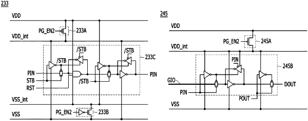
a write path control block including a first power gating circuit coupled to a supply terminal of a first voltage and a second power gating circuit coupled to a supply terminal of a second voltage, the write path control block suitable for generating a write control signal using the first and second voltages in a write mode;
a write driving block including a third power gating circuit coupled to any one of the supply terminal of the first voltage and the supply terminal of the second voltage, the write driving block suitable for transmitting a write data signal to a data input/output line using the first and second voltages based on the write control signal;
a memory block, coupled to the data input/output line, suitable for writing the write data signal or reading a read data signal;
a read path control block including a fourth power gating circuit coupled to the supply terminal of the first voltage and a fifth power gating circuit coupled to the supply terminal of the second voltage, the read path control block including a third logic circuit coupled to a supply terminal of a sixth voltage and a supply terminal of a seventh voltage, the read path control block suitable for generating a read control signal using the first and second voltages in a read mode; and
a pipe latch block including only a sixth power gating circuit having a header-only power gating structure coupled to the supply terminal of the first voltage, the pipe latch block including a fourth logic circuit coupled to any one of the supply terminal of the sixth voltage and the supply terminal of the seventh voltage, the pipe latch block suitable for latching the read data signal, which is transmitted through the data input/output line, using the first and second voltages based on the read control signal.
|