| CPC G11C 7/065 (2013.01) [G11C 7/12 (2013.01)] | 20 Claims |
|
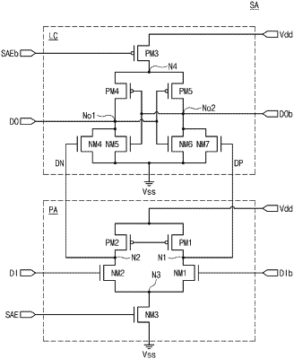
1. A sense amplifier comprising:
a pre-amplifier circuit configured to generate first internal data and second internal data, based on input data and inverted input data; and
a latch circuit configured to generate output data and inverted output data, based on the first internal data and the second internal data, wherein:
the pre-amplifier circuit includes:
a first circuit configured to provide a power supply voltage;
a second circuit configured to provide a ground voltage; and
a third circuit connected to the first circuit and the second circuit and configured to generate the first internal data and the second internal data, and
the third circuit includes:
a first NMOS transistor connected between a first node connected to the first circuit and a third node and configured to generate the first internal data and to operate in response to the second internal data;
a second NMOS transistor connected between a second node connected to the first circuit and a fourth node and configured to generate the second internal data and to operate in response to the first internal data;
a first PMOS transistor connected between a first input node receiving the input data and the third node and configured to operate in response to a sensing signal;
a second PMOS transistor connected between a second input node receiving the inverted input data and the fourth node; and configured to operate in response to the sensing signal;
a third NMOS transistor connected between the third node and a fifth node connected to the second circuit and configured to operate in response to the inverted input data;
a fourth NMOS transistor connected between the fourth node and the fifth node and configured to operate in response to the input data;
a third PMOS transistor connected between a sixth node and the first node and configured to operate in response to the sensing signal; and
a fifth PMOS transistor connected between a power node receiving the power supply voltage and the sixth node; and configured to operate in response to the sensing signal.
|