US 11,670,344 B2
Semiconductor device
Tomoaki Atsumi, Kanagawa (JP); Kiyoshi Kato, Kanagawa (JP); Tatsuya Onuki, Kanagawa (JP); and Shunpei Yamazaki, Tokyo (JP)
Assigned to Semiconductor Energy Laboratory Co., Ltd., Atsugi (JP)
Filed by SEMICONDUCTOR ENERGY LABORATORY CO., LTD., Atsugi (JP)
Filed on Dec. 2, 2021, as Appl. No. 17/540,314.
Application 17/540,314 is a continuation of application No. 16/764,955, granted, now 11,195,561, previously published as PCT/IB2018/059488, filed on Nov. 30, 2018.
Claims priority of application No. 2017-236145 (JP), filed on Dec. 8, 2017; application No. 2018-027585 (JP), filed on Feb. 20, 2018; application No. 2018-131207 (JP), filed on Jul. 11, 2018; and application No. 2018-167559 (JP), filed on Sep. 7, 2018.
Prior Publication US 2022/0093141 A1, Mar. 24, 2022
This patent is subject to a terminal disclaimer.
Int. Cl. G11C 7/04 (2006.01); G11C 5/14 (2006.01); G11C 11/4074 (2006.01); H01L 27/108 (2006.01); H01L 27/12 (2006.01); H01L 29/221 (2006.01)
CPC G11C 7/04 (2013.01) [G11C 5/14 (2013.01); G11C 11/4074 (2013.01); H01L 27/108 (2013.01); H01L 27/1225 (2013.01); H01L 29/221 (2013.01)] 6 Claims
OG exemplary drawing
 
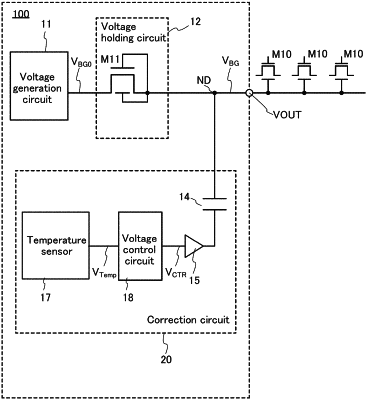
1. A semiconductor device comprising:
a transistor comprising a first gate and a second gate;
a voltage generation circuit electrically connected to the second gate of the transistor;
a capacitor, a first electrode of the capacitor is electrically connected to the second gate of the transistor; and
a voltage control circuit electrically connected to a second electrode of the capacitor,
wherein the first gate and the second gate overlap each other with a semiconductor layer therebetween, and
wherein the voltage control circuit is configured to convert a temperature information into a control voltage.