US 11,670,251 B2
Method for driving semiconductor device
Hajime Kimura, Kanagawa (JP)
Assigned to SEMICONDUCTOR ENERGY LABORATORY CO., LTD., Kanagawa-ken (JP)
Filed by SEMICONDUCTOR ENERGY LABORATORY CO., LTD., Atsugi (JP)
Filed on Sep. 14, 2022, as Appl. No. 17/944,224.
Application 17/944,224 is a continuation of application No. 17/338,465, filed on Jun. 3, 2021, granted, now 11,450,291, issued on Sep. 20, 2022.
Application 17/338,465 is a continuation of application No. 15/931,960, filed on May 14, 2020, granted, now 11,030,966, issued on Jun. 8, 2021.
Application 15/931,960 is a continuation of application No. 15/979,003, filed on May 14, 2018, granted, now 10,657,910, issued on May 19, 2020.
Application 15/979,003 is a continuation of application No. 15/148,351, filed on May 6, 2016, granted, now 9,978,320, issued on May 22, 2018.
Application 15/148,351 is a continuation of application No. 14/311,479, filed on Jun. 23, 2014, granted, now 9,343,018, issued on May 17, 2016.
Application 14/311,479 is a continuation of application No. 12/754,731, filed on Apr. 6, 2010, granted, now 8,780,034, issued on Jul. 15, 2014.
Claims priority of application No. 2009-094306 (JP), filed on Apr. 8, 2009.
Prior Publication US 2023/0005443 A1, Jan. 5, 2023
Int. Cl. G09G 3/36 (2006.01); G09G 5/10 (2006.01); G09G 3/34 (2006.01); H04N 5/208 (2006.01)
CPC G09G 3/3607 (2013.01) [G09G 3/3406 (2013.01); G09G 3/36 (2013.01); G09G 3/3614 (2013.01); G09G 3/3685 (2013.01); G09G 5/10 (2013.01); G09G 3/3413 (2013.01); G09G 2300/0452 (2013.01); G09G 2320/0233 (2013.01); H04N 5/208 (2013.01)] 10 Claims
OG exemplary drawing
 
1. A liquid crystal display device comprising:
a first light source;
a second light source;
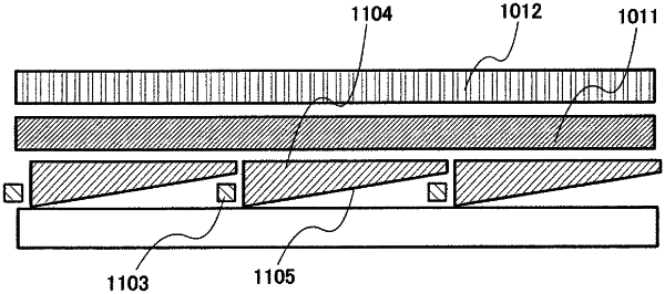
a first light guide plate over the first light source;
a second light guide plate over the second light source;
a diffusing plate over the first light guide plate and the second light guide plate; and
a display panel over the diffusing plate, the display panel comprising a transistor and a liquid crystal element,
wherein the first light source overlaps with an edge portion of the first light guide plate,
wherein the second light source overlaps with an edge portion of the second light guide plate, and
wherein a bottom surface of each of the first light guide plate and the second light guide plate has an unevenness surface.