| CPC G09G 3/3233 (2013.01) [G09G 3/3258 (2013.01); H01L 27/3262 (2013.01); H01L 27/3276 (2013.01); H01L 51/0097 (2013.01); G09G 2300/0819 (2013.01); G09G 2320/0257 (2013.01); H01L 27/124 (2013.01); H01L 27/1222 (2013.01); H01L 29/78648 (2013.01); H01L 29/78675 (2013.01); H01L 2251/5338 (2013.01)] | 20 Claims |
|
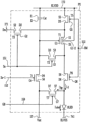
1. An organic light emitting diode display, comprising:
a substrate;
a pixel disposed on the substrate;
a scan line;
a data line;
a driving voltage line; and
an initialization voltage line,
wherein the scan line, the data line, the driving voltage line, and the initialization voltage line are connected to the pixel,
wherein the pixel comprises:
an organic light emitting element;
a first switching transistor connected to the scan line;
a driving transistor that applies a current to the organic light emitting element; and
a compensation transistor that compensates an operation of the driving transistor,
wherein the driving transistor comprises:
an overlapping layer; and
a semiconductor layer comprising a channel,
wherein the compensation transistor comprises:
a semiconductor layer comprising a channel;
a first gate electrode disposed on the semiconductor layer of the compensation transistor; and
a second gate electrode disposed under the semiconductor layer of the compensation transistor,
wherein the overlapping layer of the driving transistor is disposed between the semiconductor layer of the driving transistor and the substrate and
wherein the overlapping layer of the driving transistor receives a driving voltage that flows to the driving voltage line.
|