| CPC G09G 3/3233 (2013.01) [G09G 2320/029 (2013.01); G09G 2320/0233 (2013.01); G09G 2320/0276 (2013.01); G09G 2320/041 (2013.01); G09G 2320/045 (2013.01); G09G 2320/048 (2013.01)] | 19 Claims |
|
1. A display device, comprising:
a display panel including a plurality of pixels divided into a plurality of pixel blocks;
a data driver configured to supply a driving signal to each of the plurality of pixels and sense electrical characteristics of each of the plurality of pixels; and
a degradation compensation circuit configured to compensate input data corresponding to each of the plurality of pixels, based on a compensation rate of the pixels corresponding to the input data, and provide the compensated input data to the data driver,
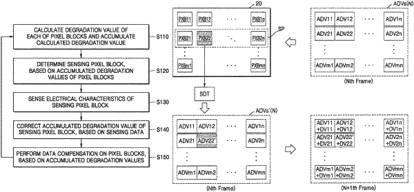
wherein the degradation compensation circuit is further configured to generate and accumulate a degradation value for each of the plurality of pixels, based on driving data corresponding to the driving signal supplied to each of the plurality of pixels, calculate a compensation rate for each of the plurality of pixels by using each pixel's accumulated degradation value and a degradation model, and correct the accumulated degradation value for each of the plurality of pixels, based on the sensed electrical characteristics,
wherein the degradation compensation circuit is further configured to
generate a plurality of accumulated degradation values corresponding to the plurality of pixel blocks, identify a pixel block having a highest accumulated degradation value of the plurality of pixel blocks as a sensing pixel block, control the data driver to sense the sensing pixel block, perform data compensation on the sensing pixel block using the corrected accumulated degradation value associated with the highest accumulated degradation value and perform data compensation on the remainder of the pixel blocks using their associated accumulated degradation values.
|