| CPC G09G 3/32 (2013.01) [G09G 2300/0426 (2013.01); G09G 2300/0819 (2013.01); G09G 2300/0842 (2013.01); G09G 2310/0267 (2013.01); G09G 2310/0275 (2013.01); G09G 2310/061 (2013.01); G09G 2310/08 (2013.01); G09G 2320/0242 (2013.01); G09G 2330/028 (2013.01)] | 16 Claims |
|
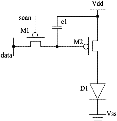
1. A pixel circuit, comprising a data write module, a storage module, a drive module and a light emitting device; wherein
the drive module comprises a first control terminal and a second control terminal; the data write module is configured to write, at a data write stage, a data signal into the first control terminal of the drive module, the storage module is configured to maintain a potential of the first control terminal, the second control terminal is electrically connected to a pulse-width modulation (PWM) signal input terminal of the pixel circuit, and is configured to control the drive module to provide discontinuous drive current according to a PWM signal input from the PWM signal input terminal at a light emission stage, and the light emitting device emits light in response to the discontinuous drive current.
|