| CPC G09G 3/32 (2013.01) [G09G 3/2092 (2013.01); G09G 3/3233 (2013.01); G09G 3/36 (2013.01); G09G 3/3648 (2013.01); G09G 2310/0205 (2013.01); G09G 2310/027 (2013.01); G09G 2310/0278 (2013.01); G09G 2310/061 (2013.01); G09G 2310/062 (2013.01); G09G 2320/0252 (2013.01); G09G 2320/0257 (2013.01); G09G 2320/0261 (2013.01); G09G 2320/0295 (2013.01); G09G 2320/043 (2013.01); G09G 2320/0673 (2013.01); G09G 2330/021 (2013.01)] | 12 Claims |
|
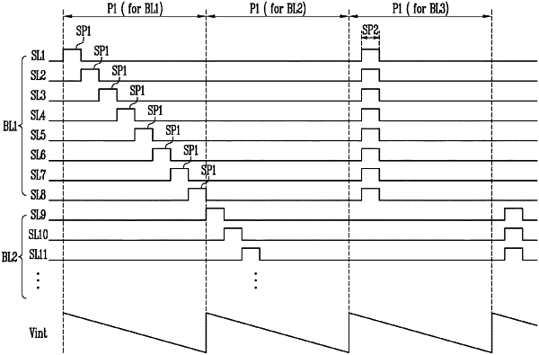
1. A display device comprising:
pixel blocks each including consecutive pixel rows connected to scan lines, control lines, and data lines, the pixel rows including pixels;
a scan driver configured to supply a scan signal to the scan lines and to supply a control signal to the control lines;
a data driver configured to supply an image data voltage or a low grayscale data voltage to the data lines; and
a power supply configured to supply a reference voltage to the pixels,
wherein a change of the reference voltage is repeated for each of the pixel blocks,
the reference voltage supplied to a first pixel row of each of the pixel blocks is greater than the reference voltage supplied to a last pixel row of each of the pixel blocks in a first scan period,
the reference voltage supplied to the last pixel row of a p-th pixel block, where p is a positive integer, is less than the reference voltage supplied to the first pixel row of a (p+1)-th pixel block, and
the last pixel row of the p-th pixel block and the first pixel row of the (p+1)-th pixel block are adjacent to each other.
|